Opened a laboratory in Todoroki, Setagaya, Tokyo (foundation)
Challenge
Conducted research on photofabrication technologies for glass and conductive films
1969
Moved to Tomigaya (current Head Office)
1969
Manufactured disks for optical encoders
1970
Dawn of a New Era
Advances made in liquid crystal technology as displays for watches and calculators
1970
Reorganized as a corporation
1976
Hatsudai Factory completed
1970
Developed patterning technology essential for liquid crystal displays. Used in many products
1978
Increased uptake of solar cells with the development of thin, flexible substrates
1980
Growth and Advancement
Debut of color LCDs
1983
Kiso Factory completed; Techno Print Co., Ltd. established
1985
Tomigaya Head Office completed
1988
Atsugi Development Center completed (now Atsugi Micro Co., Ltd.)
1981
IBM PC (IBM) released
1983
Manufactured resistive membrane touch panels
1984
Macintosh (Apple) released
1987
Developed technology for color filter substrates resistant to heat and fading. As the first in the world to successfully commercialize them for PC LCD displays, this ushered in the era of color LCDs.
Developed glass touch panels resistant to scratches and dirt
1994
Started mass production of color filter substrates
Internet increased in popularity and PCs became more advanced
1995
Windows 95 (Microsoft) released
1998
Our independently developed glass touch panels for car navigation systems were used by leading domestic manufacturers and put into mass production. Valued for its high reliability, glass then became the mainstream material for automotive touch panels.
Production of LCD products moved overseas, and domestic demand dropped
i-mode (NTT DOCOMO) released
2000
The Touch Panel Era
Spread of broadband
2000
Succeeded in developing technology for reflective color filter substrates that do not require a backlight. Capable of substantially reducing power consumption, this technology was adopted for mobile phone handsets made by major manufacturers.
Advances in AI technology through machine learning
2007
July spin-off (Kiso, Kisokoma, Atsugi)
2008
Obtained ISO 9001 certification
2007
iPhone (Apple) released
2007
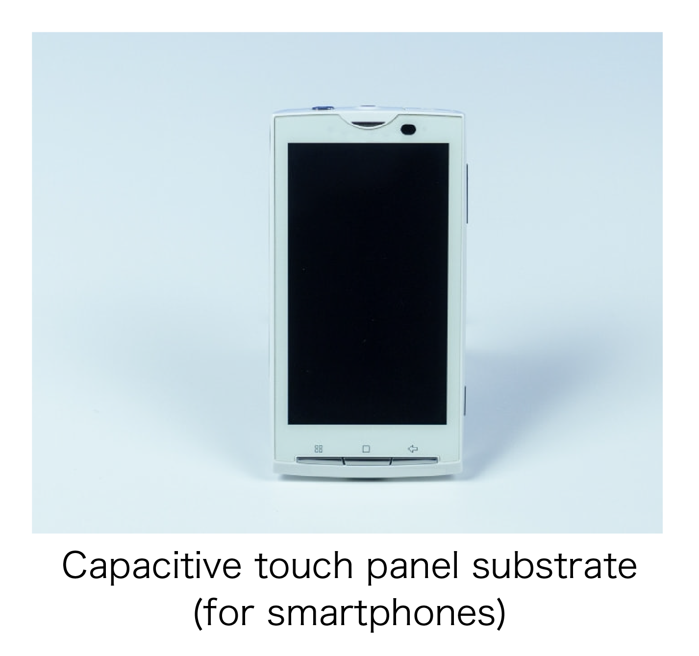
Developed capacitive touch panel technology to support multifunction smartphone features. Used in wildly popular models that symbolized the dawn of the smartphone era.
2009
Started development of micro wiring substrates leveraging thin-film processing technology
2010
Exploring New Domains
Explosive spread of smartphones and further advances in AI technology
2011
Nagaoka Factory completed
2013
Obtained ISO 14001 certification
2014
Nagaoka 2nd Factory completed
2011
Developed touch panels integrated with cover glass
2015
Started mass production of cover glass integrated touch panels for smartphones, offering excellent durability and transmittance. MICRO's technical capabilities, able to meet stringent technical requirements, received highly acclaim.
2015
Succeeded in developing processing technology to produce curved glass without any distortion. This technology contributed to the major success of groundbreaking curved automotive displays.
2019
Embarked on R&D into glass micro substrates envisioned for next-generation semiconductors
2020
Toward New Challenges
5G services launched, accelerating DX and IoT throughout society
2020
Obtained IATF 16949 certification
2023
Began development of TGV (Through-Glass Via) technology envisioned for glass core substrates, a key to achieving next-generation semiconductors. The glass processing technology that MICRO cultivated drew intense attention from around the world.